The Fastest delivery ability of high precision PCB manufacturer !
Language:

Home / All / Rigid PCB Manufacturing / Single Sided PCB Manufacturing /
PCB prototype manufacturer:Customized Single Layer PCB&Printed Circuit Board
PCB prototype manufacturer:Customized Single Layer PCB&Printed Circuit Board
| Categories | Single Sided PCB Manufacturing |
|---|---|
| Brand | PCBQuick PCB Manufacturing and Assembly |
| Model | KF-single layer pcb3 |
| Material | FR4 |
| Board Thickness | 1.6mm |
| Copper Thickness | 50um |
| Soldermask Color | Green |
| Silkscreen Color | Black |
| Surface Technics | HAL-Free |
| Min Holes | 0.2mm |
| Min Line Width and space | 5mil/5mil |
| FOB port | Shenzhen,Hongkong |
| Terms of Payment | L/C, D/A, D/P, Western Union, MoneyGram, T/T, Paypal |
| Download DOC |  |
| Update Time | Apr 28,2024 |
Detail Information
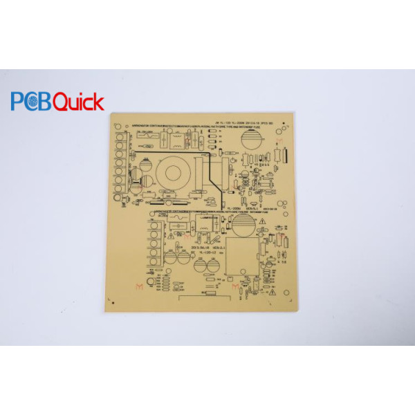
Customized Single Layer PCB Printed Circuit Board Design
Product Description
Material: FR4
Board Thickness: 1.6mm
Copper Thickness: 50um
Soldermask Color: Red
Silkscreen Color: White
Surface Technics: HAL-Free
Min Holes:0.2mm
Min Line Width and space:5mil/5mil
FR4 Made Ability
| NO | Item | Craft Ability |
|---|---|---|
| 1 | Surface Finishh | HASL,Immersion Gold,Gold Plating,OSP,Immersion Tin,etc |
| 2 | Layer | 2-30 layers |
| 3 | Min. Line Width | 3 mil |
| 4 | Min. Line Space | 3 mil |
| 5 | Min. Space between Pad to Pad | 3 mil |
| 6 | Min.Hole Diameter | 0.10 mm |
| 7 | Min. Bonding Pad Diameter | 10 mil |
| 8 | Max. Proportion of Drilling Hole and Board Thickness | 1:12:5 |
| 9 | Max. Size of Finish Board | 23 inch*35 inch |
| 10 | Rang of Finish Board's Thickness | 0.21-7.0 mm |
| 11 | Min. Thickness of Soldermask | 10 um |
| 12 | Soldermask | Green,Yellow,Black,White,Red,Transparent photosensitive solder mask,Strippable solder mask |
| 13 | Min. Linewidth of Idents | 4 mil |
| 14 | Min. Height of Idents | 25 mil |
| 15 | Color of Silk-screen | White,Yellow,Black |
| 16 | Date File Format | Gerber file and Drilling file,Report series,PADS 2000 series,Powerpcb series,ODB++ |
| 17 | E-testing | 100% E-Testing:High Voltage Testing |
| 18 | Material for PCB | High TG Material:High Frequence (ROGERS,TEFLON,TADONIC,ARLON):Halogen-free Material |
| 19 | Other Test | Impedance Testing,Resistance Testing,Microsection etc |
| 20 | Special Technological Requirement | Blind&Buried Vias and High Thickness Copper |
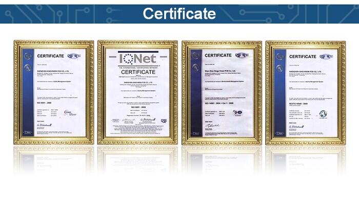
PCB Certificates
UL, TS16949, ISO14001, ISO9001-2008, and RoHS
Related Products


Please send your message to us
- *Title
- *Content
CONTACT US
- Name:
- Mary
- Tel:
86-0755-29518736
- Email:
- mary@kfquickpcb.com
- WhatsApp:
- https://wa.me/8613632989860
- Skype:
- Skype:pcbquick
- Address:
- Building D, Xintai Industrial Park, Xitou Second Industrial Zone, SongGang Town,Bao'an,Shenzhen,China
FOLLOW US
Please send your message to us
- *Title
- *Content
MOBILE WEB
Focus on mobile phone clients
QR code

subscription