The Fastest delivery ability of high precision PCB manufacturer !
Language:

Home / PCB Copy & PCB Design
PCB copy board in the case of existing PCB circuit board cloning, prototyping, component replacement, production BOM list, export schematic diagrams, etc. PCBQuick clones the circuit board, including PCB blank board clone (provide PCB files, BOM list and schematics), Also provides PCB manufacturing, component purchase and assembly.
PCBQuick PCB copy board advantages:
1. Have a professional team and engineers have more than 10 years of actual combat experience
2. Serving electronic circuit board cloning and prototyping in all walks of life
3 For a variety of blind buried hole multiple copy board short cycle, saving customers time, reduce costs
4. Solve the problem of early shutdown of factory production
5. Ensure that the cloned product and the customer provide a 100% consistent model
PCBQuick PCB copy board provides software format files: PowerPCB, Protel99/Se, PAD2000 and so on.
PCBQuick PCB copy board project consulting process:
1. Provide chip print pictures and board size, price evaluation
2. Price confirmation, send samples
3. Receive physical samples, final confirmation prices, prepaid project costs
4. Start copying the PCB
5. We provide PCB copy board documents, bill of materials, schematics, customer confirmation
6. Start PCB production
7. If the customer requests PCBA production, after the electronic whiteboard BOM table comes out, conduct the PCBA quotation
8. Price confirmation at the same time purchase components.
9. Finalize: PCB copy board + PCB production + component purchase + PCBA assembly
PCB layout design
With professional PCB design concept, excellent PCB LAYOUT team and strict design process, the company provides customers with high-quality and high-quality services. The company provides PCB impedance calculation and lamination design for customers free of charge; We support mainstream design tools: Cadence/Allegro, Pads, Altium, etc. Schematic tool support: CIS/ORCAD, Protel DXP, Design Capture, etc.
Information required for PCB design:
1. Schematic diagram: Complete electronic document format that can generate correct network table;
2. Mechanical dimension: provide identification of specific position and direction of positioning device and identification of specific height limit position area;
3. Equipment packaging: Provide equipment packaging library or electronic material specifications;
4. Wiring guidelines: describe specific requirements for special signals and design requirements for impedance and lamination.
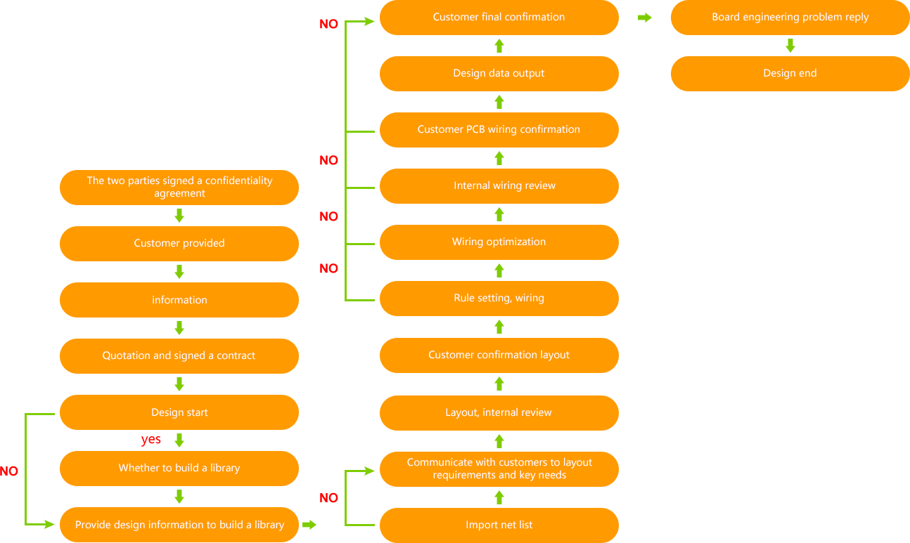
The design process
Design parameters
|
Top
|
unlimited
|
Maximum Design PIN
|
60000
|
|
Maximum Number of Connections
|
42000
|
Minimum Line Width
|
2.5 million
|
|
Minimum Line Spacing
|
2.5 million
|
Smallest Hole
|
4mil (radius perforation)
|
|
Maximum number of BGA
|
10
|
Minimum BGA PIN pitch
|
0.4mm
|
Maximum BGA PIN code | 4200 | Maximum number of networks | 15000 |
Design lead time
|
Pin number
|
0-1000
|
Design lead time (working days)
|
3-5 days
|
|
2000-3000
|
5-8 days
|
||
|
4000-5000
|
8-12 days
|
||
|
6000-7000
|
12-15 days
|
||
8000-9000 | 15-18 days | ||
10000-12000 | 18-20 days | ||
13000-15000 | 20-22 days | ||
16000-18000 | 22-25 days | ||
18000-20000 | 25-30 days | ||
Limit due date function | 10000Pin / 7 days | ||
PS: The above delivery period is the regular delivery period. It is necessary to fully evaluate the accurate design lead time based on the number of components of the circuit board, the difficulty level, the number of layers and other factors! | |||
CONTACT US
- Name:
- Mary
- Tel:
86-0755-29518736
- Email:
- mary@kfquickpcb.com
- WhatsApp:
- https://wa.me/8613632989860
- Skype:
- Skype:pcbquick
- Address:
- Building D, Xintai Industrial Park, Xitou Second Industrial Zone, SongGang Town,Bao'an,Shenzhen,China
FOLLOW US
Please send your message to us
- *Title
- *Content
MOBILE WEB
Focus on mobile phone clients
QR code

subscription