The Fastest delivery ability of high precision PCB manufacturer !
Language:

Home / Power Inverter & UPS application
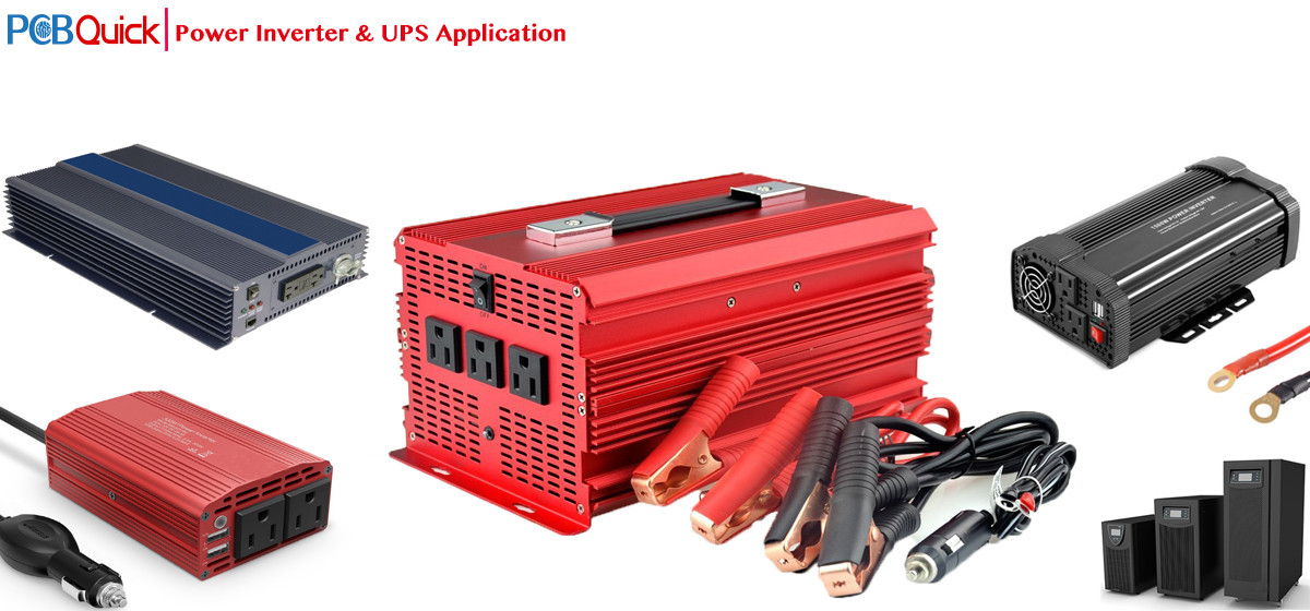
Introduction to Power Inverter & UPS
Power Inverter & UPS(Uninterruptible Power System/Uninterruptible Power Supply) has been widely used in: Mining, aerospace, industrial, computer, communications, defense, hospital business terminal, network, server, network equipment, data storage equipment, UPS uninterruptible power supply emergency lighting system, railways, shipping, transportation, power plants, substations, power plant, fire security alarm system, wireless communication system, program-controlled switches, mobile communications, solar energy storage energy conversion equipment, control equipment and emergency protection system, personal computer, and many other fields.
As the status of information industry in the national economy more and more important, the world will further increase the investment in construction industry especially the information industry, the downstream areas speed up the pace of informationization construction, must also drive the market demand for Power makes & UPS. However, with the increase of Power consumption, the shortage of machine room area and the increasing demand of low energy consumption, high efficiency and high reliability of Power Inverter & UPS technology have attracted much attention. Increasingly saturated market for Power makes & UPS also puts forward the new requirements: high Power/modular, high frequency, digital, intelligent, networked, and energy conservation and environmental protection. The Power makes & UPS industry increasingly fierce competition, the construction of brand and high-end custom is particularly important.
The effect of Copper PCB on the Power Inverter & UPS
The most basic requirement of Power Inverter & UPS for circuit boards is that the copper sheet is thicker than normal and can withstand high current without affecting signal transmission. Thick copper printed circuit board is made of thick copper foil and super thick copper foil printed circuit board. The thickness of the copper foil is usually 18um, 35um, 55um, and 70um. The most commonly used thickness of the copper foil is 35um. The plate with copper thickness beyond the normal range is called thick copper plate.
1. Hazards to Power Inverter & UPS due to low-price and low-quality copper circuits:
(1) Excessive current intensity will affect signal transmission
(2) A strong current will break through the thin copper
(3) The copper thickness is not up to standard and the heat dissipation is poor, which will cause a fire.
(4) If there is any problem in the warranty period, the after-sales warranty fee will be increased; College (5), let you lose customer trust, loss of customers.
2. Advantages of the PCBQuick high-quality thick copper circuit board to Power Inverter & UPS products:
(1) Can carry a large current and high voltage
(2) High heat conduction ensures stable operation of products;
(3) To improve the warranty period so as to improve the competitiveness of the product market and reduce the after-sales warranty expenses;
(4) Increase customer trust and stabilize customers.
Important factors affecting Power Inverter & UPS!
PCBQuick's basic requirements for thick copper circuit boards:
1. During the production process, the engineer calculates the line current carrying a value of copper berthing thickness, line width and line distance (specifically, check the PCB design copper platinum thickness, line width, and current relationship).
2. Process parameters are monitored in the production process
3. Add a certain value according to the area value calculated by the computer and the empirical constant accumulated in actual production;
4. According to the calculation of current value, in order to ensure the integrity of hole plating, we must increase a certain value in the original electric flow numerical impact current, and then back to the original value in a short time;
5. When the PCB plating reaches 5 minutes, take out the base plate and observe whether the copper layer on the surface and the inner wall of the hole is complete.
6. A certain distance must be maintained between the substrate and the substrate;
7. When the thickness of copper plating reaches the required plating time, a certain amount of current shall be maintained during the removal of the substrate to ensure that no blackening or darkening will occur on the surface and holes of the subsequent substrate.
PCBQucik’s helps your Power Inverter & UPS!
PCBQuick has been focusing on the design and production of thick copper circuit boards for many years and has summarized its own production experience:
The main purpose of thickening copper plating is to ensure that the copper coating is thick enough in the hole and the resistance value is within the range of the technical requirements.
1. preparation and inspection of plating treatment before plating
(1). Mainly check the metallization quality of the hole, and make sure there are no residual objects, burrs, black holes, holes, etc.;
(2). Check whether there is any dirt and other surplus on the surface of the substrate;
(3). Check the number, drawing number, process documents and process description of the substrate;
(4). Clear the mounting parts, mounting requirements and coating area that the plating tank can withstand;
(5). The coating area and process parameters should be clearly defined to ensure the stability and feasibility of plating process parameters;
(6). The cleaning and preparation of the conductive parts and the first electrification treatment make the solution appear to be activated;
(7). Determine whether the tank liquid component is qualified and the surface area of the plate is in the state; If a spherical anode is used, the consumption must be checked.
(8). Check the firmness of the contact area and the range of voltage and current fluctuations.
2. Quality control of thickened copper plating
(1). The accurate calculation of plating area and the impact on the current reference for the practical production process, the right to determine the current required values, grasp the current changes in the electroplating process, to ensure the stability of plating process parameters;
(2). Before plating, the commissioning plate is firstly used for trial plating, so that the tank liquid is activated;
(3). Determine the direction of the total current flow, and then determine the order of the hanging plate. Ensure the uniformity of the current distribution to any surface;
(4). Ensure the uniformity of the plating layer in the hole and the consistency of the thickness of the plating layer. In addition to the technological measures of stirring filtration, shock current should be adopted.
(5). Constantly monitor the changes of current during plating to ensure the reliability and stability of current value;
(6). Check whether the thickness of the copper plating layer of the hole meets the technical requirements.
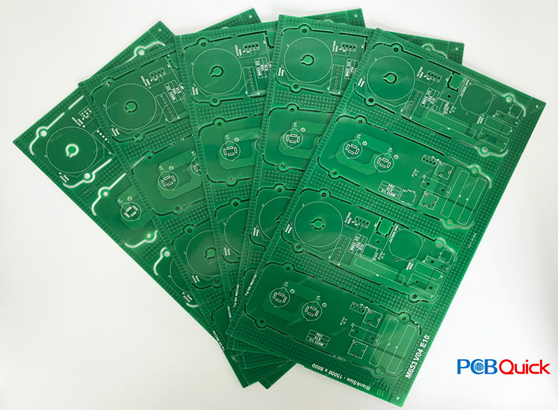
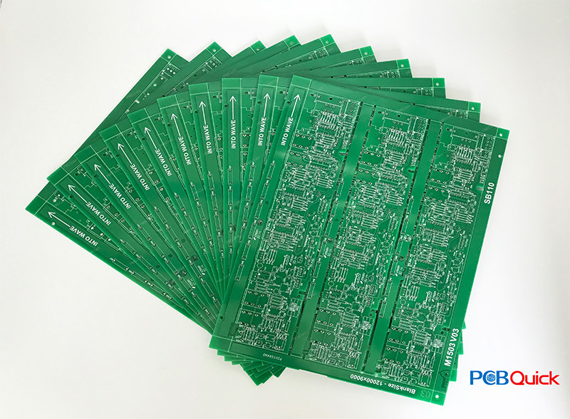
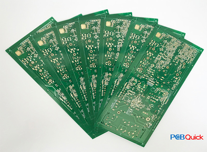
PCBQuick’s Cooper PCB application case!
Based on good quality do endorsement, PCBQuick thick copper circuit board gradually obtained excellent reputation. Our thick copper circuit board is applied to the comprehensive: weapon control system, radar system power supply, high power planar transformer winding, switchboard, battery charging and monitoring system.
Thick copper circuit board
Material: FR4 2layer
Board Thickness: 1.6mm
Copper Thickness: 70um
Solder mask Color: Green
Silkscreen Color: White
Surface Technics: HAL-Free
Min Holes:0.3mm
Min Line space and width: 8/8mil
Heavy Copper PCB
Material: FR4 4layer
Board Thickness: 1.6mm
Copper Thickness: 105um/70um/70um/105um
Solder mask Color: Green
Silkscreen Color: White
Surface Technics: HAL-Free
Min Holes:0.3mm
Min Line width and space: 12/10mil
Extreme copper pcb
Material: FR4 2layer
Board Thickness: 2.0mm
Copper Thickness: 135um
Solder mask Color: Green
Silkscreen Color: White
Surface Technics: ENIG
Min Holes:0.3mm
Min Line width and space: 12/10mil
PCBQuick to save your time and earn market!
PCBQuick Videos:
PCBQUICK
Are you still worrying about the LED strip custom service?
PCBQUICK
KingFung International Limited Video
PCBQUICK
I`m sure this is the FPC Process flow that you don`t know!
PCBQUICK
CNC Fascia Plate Process
CONTACT US
- Name:
- Mary
- Tel:
86-0755-29518736
- Email:
- mary@kfquickpcb.com
- WhatsApp:
- https://wa.me/8613632989860
- Skype:
- Skype:pcbquick
- Address:
- Building D, Xintai Industrial Park, Xitou Second Industrial Zone, SongGang Town,Bao'an,Shenzhen,China
FOLLOW US
Please send your message to us
- *Title
- *Content
MOBILE WEB
Focus on mobile phone clients
QR code

subscription