The Fastest delivery ability of high precision PCB manufacturer !
Language:

Home / All / Rigid PCB Manufacturing / Single Sided PCB Manufacturing /
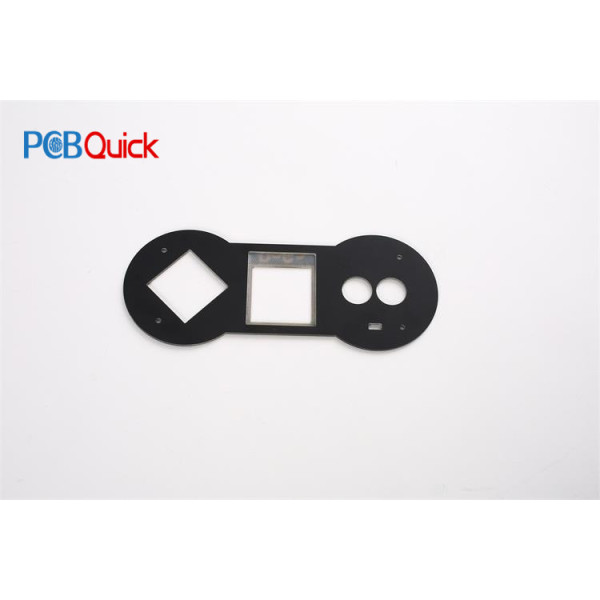
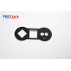
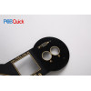
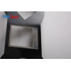
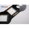
Single layer pcb manufacturing process:Double Sided Soldermask With Plating Copper Word
Single layer pcb manufacturing process:Double Sided Soldermask With Plating Copper Word
| Categories | Single Sided PCB Manufacturing |
|---|---|
| Brand | PCBQuick PCB Manufacturing and Assembly |
| Model | KF-01 |
| Material | FR4 |
| Board Thickness | 1.6mm |
| Copper Thickness | 35um |
| Soldermask Color | Black |
| Silkscreen Color | White |
| Surface Technics | ENIG |
| Min Holes | 0.2mm |
| Min Line Width and space | 5mil/5mil |
| FOB port | Shenzhen,Hongkong |
| Terms of Payment | L/C, D/A, D/P, Western Union, MoneyGram, T/T, Paypal |
| Download DOC |  |
| Update Time | Apr 28,2024 |
Detail Information
Single layer pcb manufacturing process:
On a typical PCB, the characters we see are usually painted in plain paint. However, some special circuit boards use copper as raw material for character marking.
A function of printing characters in copper is simply to look good. Use as nonferrous metal in product labeling can indirectly improve product image and brand value.
Another function of copper screen printing is to open the window in the stratum. As the foundation of electronic products, it links each component and keeps the current unobstructed. However, it is inevitable to generate heating in the working engineering. If the excessive heat cannot be spread out, it will not only hinder the current seriously, but also burn the circuit and cause damage. So the designers came up with an ingenious way of making the copper layer directly exposed to the air, which would allow it to dissipate heat more efficiently. So the designers combined the silk-layer characters on the surface of the printing plate to create a new process that combines thermal and expressive features - ground windowing.This technique is particularly common in high-power electronics。
Maybe it’s helpful to you:


Web link:
Related Products


Please send your message to us
- *Title
- *Content
CONTACT US
- Name:
- Mary
- Tel:
86-0755-29518736
- Email:
- mary@kfquickpcb.com
- WhatsApp:
- https://wa.me/8613632989860
- Skype:
- Skype:pcbquick
- Address:
- Building D, Xintai Industrial Park, Xitou Second Industrial Zone, SongGang Town,Bao'an,Shenzhen,China
FOLLOW US
Please send your message to us
- *Title
- *Content
MOBILE WEB
Focus on mobile phone clients
QR code

subscription