The Fastest delivery ability of high precision PCB manufacturer !
Language:

Home / Special board and process
Due to the shape or performance of the product, sometimes the PCB board will be affected. Special processes and production processes are needed to meet assembly and performance requirements. So let's do a little bit of an introduction here.
Surface treatment:
1.ENIG,Chem.Ni/Au;Immersiom Gold
2.Plating Gold,Flash Gold
3.HAL(leed-free)
4.HAL(leed)
5.Chem.Tin
6.Chem.Ag
7.OSP
8.Gold finger
ENIG- is called Electroless Nickel/Immersion Gold, which is a kind of surface treatment technology of PCB.
ENIG has the following characteristics:
1. Smooth surface (relatively tin spraying, etc.);
2. Good heat dissipation and solderability;
3. Long storage time (more than 1 year in vacuum packaging);
4. SMT process can withstand multiple backflow welding, but heavy industry can be repeated.
5. The thickness of common nickel plate is generally 120-200u", and the thickness of gold plate is 1-5u"; Generally, the thickness of the alloy wire is more than 10u", and the thickness of nickel is more than 150u".
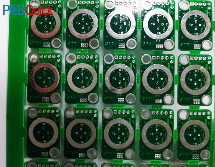
Special process of hole:
From the perspective of function, perforation can be divided into two types: first, it is used for electrical connection between each layer; Second, it is used for fixing or positioning the device.
In the process, these holes are usually blind via, buried via and through via. The blind hole is located on the top and bottom surface of the printed circuit board and has a certain depth. It is used for the connection between the surface line and the inner layer line below. buried via refers to the connection hole in the inner layer of the printed circuit board, which will not extend to the surface of the printed circuit board. Both of the above types of holes are located in the inner layer of the circuit board. Before lamination, the holes are formed by the through-hole forming process. The third is called a through-hole, which passes through the entire circuit board and can be used to interconnect internally or as an installation and positioning hole for components. Because the through-hole is easier to realize in the process and the cost is lower, it is used in most PCB instead of the other two kinds of through-hole.
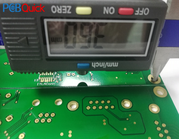
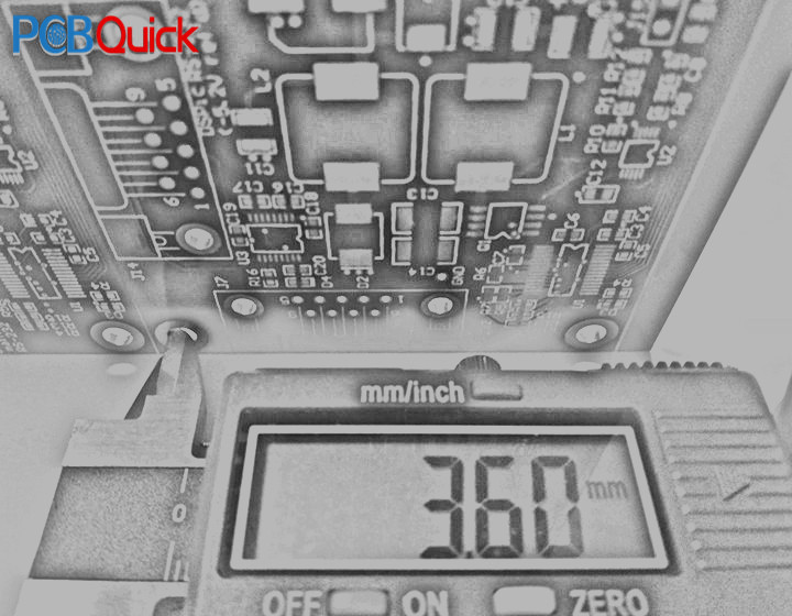
PTH(plated through hole)
Aperture tolerance minimal:
±0.075mm
Slot minimum tolerance:
L±0.15mm W±0.10mm
through via hole
Slot cutter diameter(min):
0.5mm
Drilling aperture(max):
6.5mm
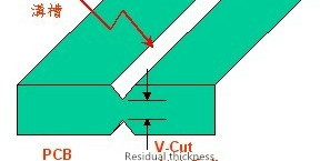
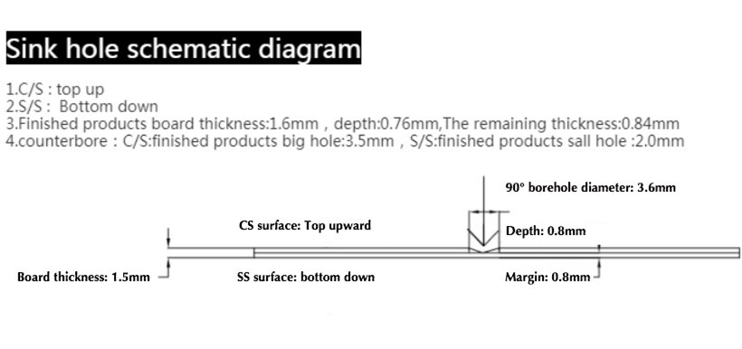
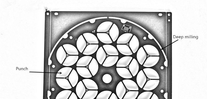
Cutting of plate:
Maybe it’s helpful to you:
Web link:
CONTACT US
- Name:
- Mary
- Tel:
86-0755-29518736
- Email:
- mary@kfquickpcb.com
- WhatsApp:
- https://wa.me/8613632989860
- Skype:
- Skype:pcbquick
- Address:
- Building D, Xintai Industrial Park, Xitou Second Industrial Zone, SongGang Town,Bao'an,Shenzhen,China
FOLLOW US
Please send your message to us
- *Title
- *Content
MOBILE WEB
Focus on mobile phone clients
QR code

subscription