The Fastest delivery ability of high precision PCB manufacturer !

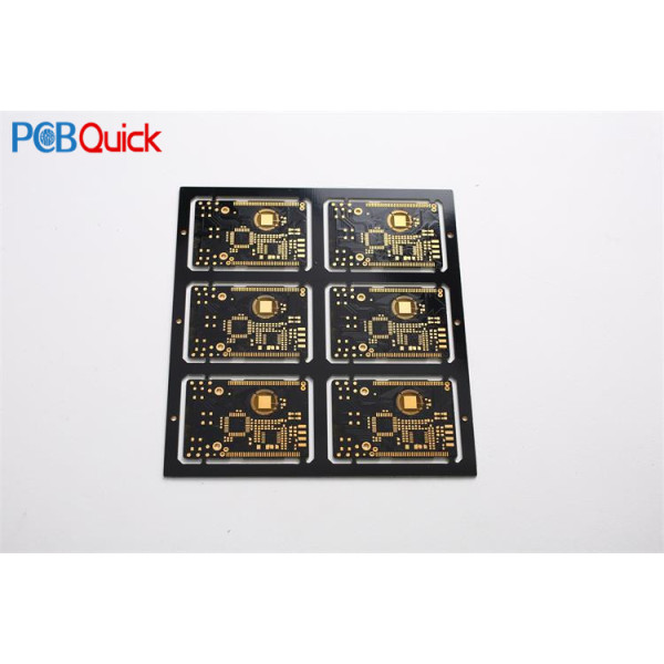
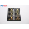
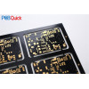
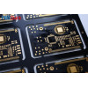
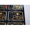
custom printed circuit pcb board with ENIG for PCBQuick
custom printed circuit pcb board with ENIG for PCBQuick
| Categories | Double Sided PCB Manufacturing |
|---|---|
| Brand | PCBQuick PCB Manufacturing and Assembly |
| Model | KF-FR4 PCB |
| Base Material | FR4 |
| Copper Thickness | 1oz |
| Board Thickness | 2.0mm |
| Min. Hole Size | 0.2mm |
| Min. Line Width | 0.1mm |
| Min. Line Spacing | 0.1mm |
| Surface Finishing | HASL/ENIG |
| Solder Mask | Black |
| Silk Screen | White |
| Unit Price | US $ 60-180 / square meter |
| FOB port | ShenZhen, HongKong |
| Terms of Payment | L/C, D/A, D/P, Western Union, MoneyGram, T/T, Paypal |
| Download DOC |  |
| Update Time | Apr 25,2024 |
custom printed circuit pcb board with ENIG for PCBQuick
FR4 2.0mm double-sided pcb board
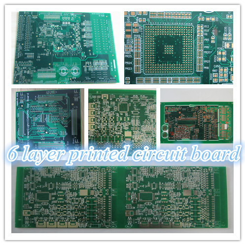
Layers: 1-20 layer
Material:FR4
Board thickness:1.6mm
Copper Thickness: 35um
Min Holes:0.2mm
Min Line Width and space:5mil/5mil
Slodermask Color:Black
Silkscreen: White,
Surface finish:ENIG
Outline: Routing & V-CUT
Plus Test Point on Technology side
1.Printed Circuit Board Fabricate/Assembly
2.UL,SGS,ROHS Certificated
3.Competitive Price,High Quality
4.OEM Circuit Assembly
Welcome To K.F PCB Factory
We are professional PCB manufacturer with ten years experiences .
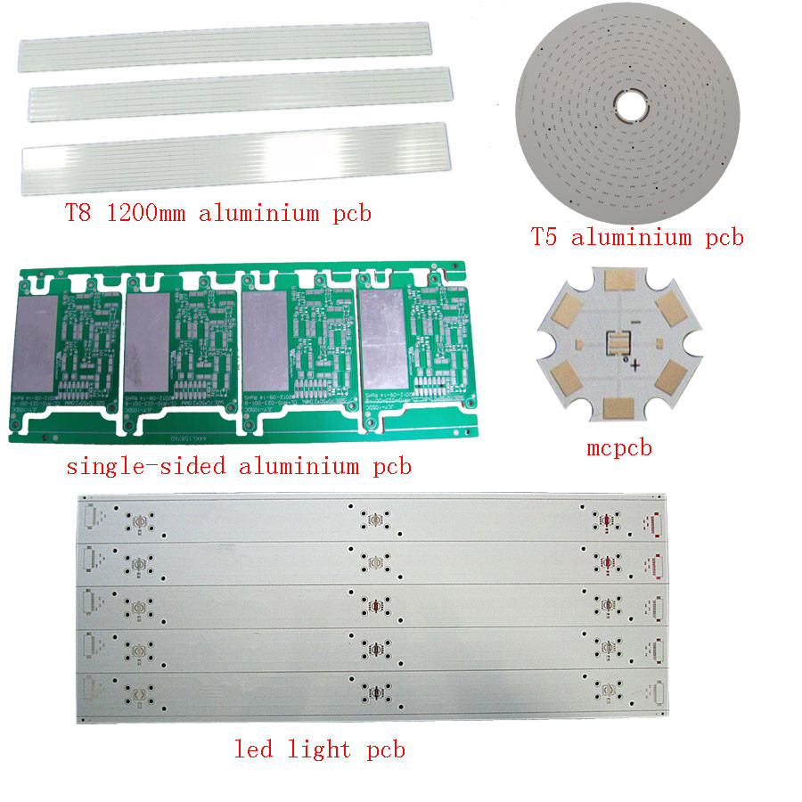
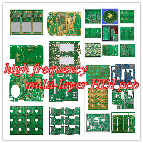
Products range-single, double side ,multi-layer PCB ,flexible PCB and MCPCB.
We can provide fast prototype service – S/S in 24hrs , 4-8layers in 48-96 working
hrs production time .
1.PCB Made Ability:
Item | Technical Standards | ||
|---|---|---|---|
Rise | 1-20 Layer | ||
Material | FR4 | ||
Board Thickness | 1.6mm | ||
Copper Thickness | 35um | ||
Soldermask Color | Green | ||
Silkscreen Color | White | ||
Min Holes | 0.2mm | ||
Surface Technics | ENIG | ||
Min Line Width and space | 5mil/5mil | ||
Outline | Routing & V-CUT | ||
Tolerance | Pore spaces | +/-0.075mm(3mil) CNC Driling | |
Line width | +/-0.05mm(2mil) or | ||
+/-20% of original artwork | |||
Aperture | PTH L:+/-0.075mm(3mil) | ||
Non-PTH L:+/-0.05mm(2mil) | |||
Appearance Tolerance | +/-0.125mm(5mil) CNC Routing | ||
+/-0.15mm(6mil) by Punching | |||
Warp | 0.70% | ||
Insulation Resistance | 10Kohm-20Mohm | ||
Conduction Resistance | <50ohm | ||
Plus Test Point on Technology side | |||
MLB | Interlaminar deviation | 4 layers:0.15mm(6mil)max | |
6 layers:0.25mm(10mil)max | |||
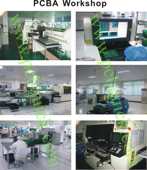
2.Detailed Terms for Pcb Assembly
Technical Requirement:
1) Professional Surface-mounting and Through-hole soldering Technology
2) Various sizes like 1206,0805,0603 components SMT technology
3) ICT(In Circuit Test),FCT(Functional Circuit Test) technology.
4) PCB Assembly With UL,CE,FCC,Rohs Approval
5) Nitrogen gas reflow soldering technology for SMT.
6) High Standard SMT&Solder Assembly Line
7) High density interconnected board placement technology capacity.
Production Requirement:
1) Gerber file and Bom list
2) PNP Files,clear pics needed for pcba
3) Testing method for products
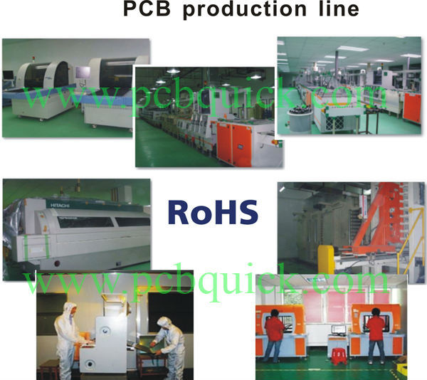
3.View of PCB(PCBA) Factory


- *Title
- *Content
- Name:
- Mary
- Tel:
86-0755-29518736
- Email:
- mary@kfquickpcb.com
- WhatsApp:
- https://wa.me/8613632989860
- Skype:
- Skype:pcbquick
- Address:
- Building D, Xintai Industrial Park, Xitou Second Industrial Zone, SongGang Town,Bao'an,Shenzhen,China
- *Title
- *Content
Focus on mobile phone clients
