
Proofing those unknown high multilayer circuit board PCB production difficulty
Proofing those unknown high multilayer circuit board PCB production difficulty
As the "core main force" of multilayer PCB in communication, medical treatment, industrial control, security, automobile, electric power, aviation, military industry, computer peripheral and other fields, the product functions are getting higher and higher, and the PCB is getting more and more precise, so it is more and more difficult to produce.
1. Difficulties in making inner circuit
Multilayer pcb line has high speed, thick copper, high frequency, high Tg value of a variety of special requirements, internal wiring and graphic size control requirements are increasingly high. For example, for ARM development board, there are many impedance signal lines in the inner layer. To ensure the integrity of impedance increases the difficulty of production of inner layer lines.
There are many signal lines in the inner layer, and the width and spacing of the lines are basically about 4mil or less. Multi - core plate layer thin production is easy to wrinkle, these factors will increase the production of inner layer.
Suggestion: the line width and distance should be designed above 3.5/3.5mil (most factories have no difficulty in production).
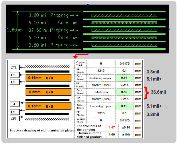
For example, the six-layer board is recommended to be designed with a false eight-layer structure, which can meet the impedance requirements of 50ohm, 90ohm and 100ohm of the inner 4-6mil line width.
2.Difficulty in alignment between inner layers
With more and more layers, the alignment requirements of the inner layer are higher and higher. The film will expand and shrink under the influence of the workshop environment temperature and humidity, and the core plate will have the same expansion and shrink when produced, which makes the alignment accuracy between the inner layer more difficult to control.
This can be trusted PCBQuick!
3. Difficulties in pressing process
Multi - core and PP (version of the cure) superposition, in the pressure of lamination, slip plate and drum residue and other problems. In the design process of the inner layer structure, the dielectric thickness between layers, the flow of glue and the heat resistance of the plate should be considered, and the corresponding pressing structure should be designed reasonably.
Suggestion: keep the inner layer evenly paved with copper, in large area without the same copper balance with PAD.
4. Difficulties in drilling production
The multilayer pcb is made of high Tg or other special boards. The roughness of the drilling is different with different materials, which increases the difficulty of removing the glue slag in the hole. High-density multilayer plate has high hole density, low production efficiency and easy to break the knife. When different networks pass through holes, the hole edge is too close, which will lead to CAF effect.
Suggestion: hole edge spacing of different networks ≥0.3mm
