
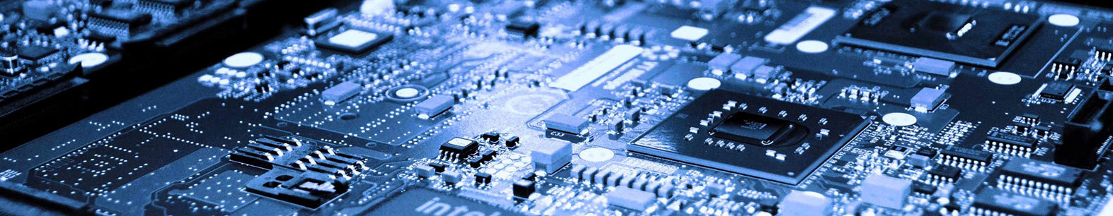
PCB Design Process
how to design pcb ?
Step 1: Design the PCB circuit with a Software
Draw the schematic circuit diagram with the PCB layout software such as CAD software, Eagle software. It is possible to change the circuit design’s position according to your convenience and requirement. Here are some procedure about Eagle software:
1.Opening your Eagle circuit board design software.
2.Appearing a window with a menu bar.
3.Clicking on the file menu.
4.Selecting ‘new design’ from the drop-down menu.
5.Clicking on the library menu.
6.Selecting ‘pick devices/symbol’ from the drop-down menu.
7.Selecting a relevant comment by double clicking on it, so that the component appears on the window.
8.Adding all the components and draw the circuit with proper connections as shown in the figure.
9.Entering the rating of each component according to the requirement.
10.Going to Command Toolbar and click Text editor varriages, click on the Varriages, and then close the window.
11.Next, there is a black screen which is the layout or the film diagram of the circuit as shown in the below figure, and save this as an image format.
Step 2: Film generation
The film is generated from the finalized circuit board diagram of the PCB layout software which is send to the manufacturing unit where the negative image or mask is printed out on a plastic sheet
Step 3: Select Raw Material
Printed circuit board is usually made with an unbreakable glass or fiberglass with copper foil bonded unto one or both the sides of the board. It is often used in household electrical devices.
Step 4: Preparing Drill Holes
There are two types of machines available to drill the PCBs, including hand machines and CNC machines. The hand machines require human intervention or effort to drill the holes, while CNC machines are controlled by computer,and also can use hand operation.
Step5: Apply Image
The laser printers are a better way to print the layouts on printed circuit boards. The following steps are used to print the PCB layout through a laser printer:
1.Taking a clean and neat copper paper and placing it on the laser printer.
2.Next, storing the designed layout film in the computer.
3.A laser printer prints the designed circuit layout on a copper paper whenever it gets a print command from the computer.
Step 6: Stripping and Etching
This process involves removing the unwired copper on the PCBs by using different types of chemicals like ferric chloride, ammonium per-sulphate, etc. Make the solvent by mixing 1% of sodium hydroxide and 10 grams of sodium hydroxide pellets to one liter of water and mix it until everything is dissolved. Next, the PCB is put on a chemical bowl and cleaned up with a brush. during this process, if the PCB is still greasy, due to applied sunflower or seed oil, the developing process may take about 1 minute.
Step 7: Testing
After finishing all pcb manufacturing process, the Board undergoes a testing process to check whether the PCB is working properly. Now ,our factory uses flying probe and frame test.
Those are descriptions and pictures of Pcb design process,if you have any other problem,please contact us as soon as possible
Maybe it’s helpful to you:
Web link
