The Fastest delivery ability of high precision PCB manufacturer !

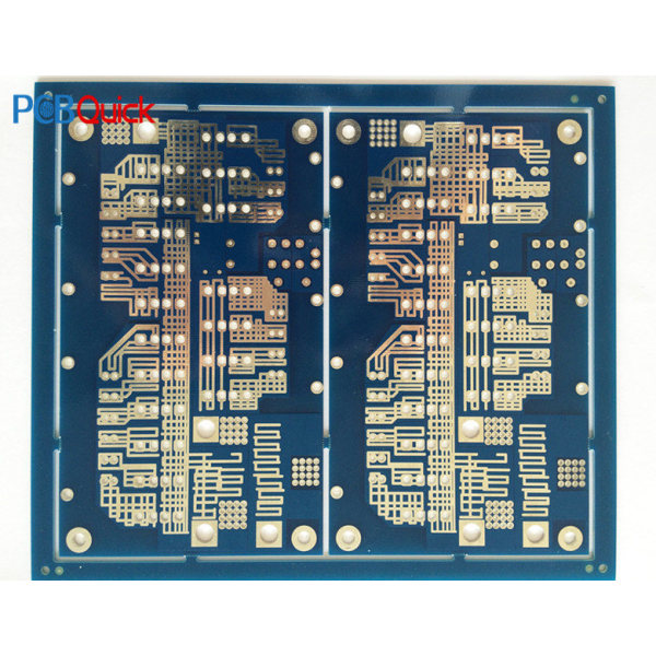
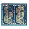
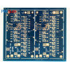
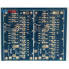
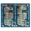
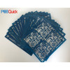
Express fabrication fr4 pcb stencil -Blue multilayer circuit board
Express fabrication fr4 pcb stencil -Blue multilayer circuit board
| Categories | Multilayer PCB Manufacturing |
|---|---|
| Brand | PCBQuick PCB Manufacturing and Assembly |
| Model | KF-FR4 PCB-12 |
| Solder mask | Blue |
| Silkscreen Color | white |
| FOB port | ShenZhen, HongKong |
| Terms of Payment | L/C, D/A, D/P, Western Union, MoneyGram, T/T, Paypal |
| Download | |
| Update Time | May 10,2025 |
NO | Item | Craft Ability |
1 | Surface Finish | HASL,Immersion Gold,Gold Plating,OSP,Immersion Tin,etc |
2 | Layer | 2-30 layers |
3 | Min.Line Width | 3mil |
4 | Min.Line Space | 3mil |
5 | Min.Space between Pad to Pad | 3mil |
6 | Min.Hole Diameter | 0.10mm |
7 | Min.Bonding Pad Diameter | 10mil |
8 | Max.Proportion of Drilling Hole and Board Thickness | 1:12:5 |
9 | Max.Size of Finish Board | 23inch*35inch |
10 | Rang of Finish Board′s Thickness | 0.21-7.0mm |
11 | Min.Thickness of Soldermask | 10um |
12 | Soldermask | Green,Yellow,Black,White,Red,transparent photosensitive solder mask,Strippable solder mask |
13 | Min.Linewidth of Idents | 4mil |
14 | Min.Height of Idents | 25mil |
15 | Color of Silk-screen | White,Yellow,Black |
16 | Date File Format | Gerber file and Drilling file,Report series,PADS 2000 series,powerpcb series,ODB++ |
17 | E-testing | 100%E-Test:High Voltage Testing |
18 |
Material for PCB | High TG Material:High Frequence(ROGERS,TEFLON,TADONIC,ARLON):Haloger free Material |
19 | Other Test | Impedance Testing,Resisitance Testing,Microsection etc |
20 | Special Technological Requirement | Blind&Buried Vias and High Thickness Copper |


- *Title
- *Content
- Name:
- Mary
- Tel:
86-0755-29518736
- Email:
- mary@kfquickpcb.com
- WhatsApp:
- https://wa.me/8613632989860
- Skype:
- Skype:pcbquick
- Address:
- Building D, Xintai Industrial Park, Xitou Second Industrial Zone, SongGang Town,Bao'an,Shenzhen,China
- *Title
- *Content
Focus on mobile phone clients
